Do You Want to Search any schema, Datasheet With Google.....? Write Keyword below

Do You Want to Search any schema, Datasheet With Google.....? Write Keyword below

Showing posts with label Audio Power Aplifier. Show all posts

400W Stereo Marshall Leach Amplifier

400W Stereo Audio Amplifier based on the original Marshall Leach involvement, but has made some improvements. Regarding the power supply voltage to the +-75V. VC comparing the performance of the modified Leach 700W/2R on one common board of both channels, as well as protection and control circuits for the fans. Compared to the 700W version a bit different in wiring. Because some things in the 700W version is completely tightened to perfection.


                                               700W version could criticize a couple of things:

1st very high gain output stage resulting in deterioration of signal noise distance. Therefore 700W version even more noisy.

2nd The absence of multipliers Ube bias current control and maintain temperature stability diagram. The 700W version of the thermal stabilization solved by a single transistor, which can sometimes cause a great loss due to power control is fast enough and has some delays. Therefore JPA400 added to this multiplier.

3rd Protection Error on board speakers, the amplifier is less comfortable and it is necessary to add this protection to the side somewhere special plate.

4th no possibility to correct the offset voltage of the amplifier output, this has a rather large weight in the differential pair of transistors and voltage level. Here this is solved by means of trimmer connected to the input Mark

5th The work points the individual stages are laid pretty low, it will also cause an increase in total harmonic distortion as well as intermodulačního distortion.


All this is in JAP400 removed. The input amplifier is Mark with adjustable offset voltage. Mark is mainly due Preamplified signal for generating the actual end-impedance amplifiers and separates. The differential amplifier is a classic symmetrical with the current 5 mA per couple, which is about 2.5 mA each transistor. Equally, shifted the operating point voltage amplifier to approximately 13 mA. This modified driver will provide enough power for generating terminal transistor and is hard enough. At the end of this time is five pairs of end-type transistor 2SC5200 / 2SA1943. Current policy is converted into the number of transistors. It has a negative slope and replicates the characteristics of SOAR terminal transistors. Current protection for amplitude limitation limits the end-around transistors 7A. As has been mentioned on the thermal stabilization of the multiplier is used Ube, is formed by two NPN and PNP transistors.


The board also includes an amplifier circuit for the fan control. This circuit ensures that the fan speed control depending on temperature. At the temperature to 65 ° C, fan runs for about 30%, it greatly reduces noise. After exceeding this temperature, the fans start running at 100% and lights to signal overtemperature. fans again at reduced power switch at about 42 ° C. Thermal protection is associated with protection of the speakers at cooler temperatures exceeding 80 ° C, the speaker is disconnected. On board is a relay switch that allows stereo / bridge mode, the indikovám LED on the front panel. The amplifier also includes an auxiliary power source to the main board, formed by transistor stabilizer. Due to higher electric circuit protection circuit and fan control. There is also an indicator of an excited, solved by the presence of the indicator signal and clip detector.

Technical parameters:

Output power:                      2x 400W/4R, 2x230W/8R
Minimum holiday zázěž:         4R
Slew rate:                             45V/us
Bandwidth:                           8-150 000 Hz /-3dB
Maximum permissible voltage: +-75V
Filter Capacity:                    2 x 20G / 80V
Sensitivity DC protection:    + /-2V
Late connection:                  2 seconds
Fusing end amplifier:            4 8 A / F
Input sensitivity for maximum excitation: 1V


The monophonic 270 watt Double barreled Amplifier

This amplifier is the monophonic 270 watt Double barreled Amplifier. For the original article, I specified plus and minus 85 V dc power supply voltages. The voltage can be increased to about 93 V to obtain a power rating of 300 W. The amplifier can be built either as a stereophonic or a monoponic unit. My original amps were mono units because the heat sinks, transformer, and filter caps that I used were too large for a stereo amp.

The circuit described on this page is a modification of the original Double Barreled Amplifier. The circuit has been simplified somewhat. The circuit board layout is smaller and much more compact. The driver transistors now mount on the circuit board instead of on external heat sinks. And the circuit has the feedforward compensation that I describe for the Low TIM Amplifier.

If you build this amplifier, you must keep the wiring between the heat sinks and the circuit boards as short as possible if you don't want oscillation problems.

When you test the circuit boards before connecting the power transistors, temporarily connect a 10 ohm resistor in series with a 0.1 ufd capacitor from the loudspeaker output to the power supply ground.
The Circuit Boards

I do not have circuit boards for the Double Barrelled Amplifier. If you wish to build it, you must make your own. Two drawings show the parts layout on the board, one with circuit traces and one without. These are scaled by a factor of 1.5. The other shows the circuit traces only. All layout views are from the component side of the board. You must flip the layout for the foil traces over to obtain the solder side view. The circuit board measures 4 inches by 6 inches. To my knowledge, there are no errors in the layout. If you decide to use it, you should carefully check it for errors because I could have easily made a mistake.

I do not recommend that you make the circuit boards unless you have experience in doing it. A source of materials for making your own printed circuits can be found here. I have been told that their "Press and Peel Blue" product (not the wet stuff they sell) can be used to successfully make boards with traces as narrow as 0.01 inch. The smallest traces on the amplifier layout are 0.03 inch wide. The PnP Blue product is basically a transfer medium that allows you to transfer the toner image from a laser printer directly onto bare copper clad board and then etch it in FeCl3 (ferric chloride).

After you etch the board, the copper should be cleaned with steel wool, lightly coated with solder flux, and then "tinned" with a soldering iron and rosin core solder. Do not use a commercial tinning solution that you dip the board into. It is almost impossible to solder a board that is tinned with one of these products because they corrode very quickly. When you drill the board, you should use the correct size drill bit for the pads. The hole diameters I recommend are: small pads - 0.032 inch, medium pads - 0.040 inch, large pads - 0.059 inch, mounting holes - 0.125 inch. If you do not use a sharp drill bit, you can pull the pads off the board when you drill it.

Circuit Description

If you compare the Double Barreled circuit to the Low TIM circuit, you will see a lot of similarity between the two. Indeed, there is a Low TIM Amplifier embedded in the Double Barreled Amplifier. The major difference between the two is that transistors are added in series with those in the Low TIM circuit to form the Double Barreled circuit. By doing this, the voltage across the transistors is decreased so that the power supply voltage can be increased for higher output power.

Basically, the circuit description for the Low TIM Amplifier also applies to the Double Barreled Amplifier. The major difference between the two is the addition of transistors Q22 through Q31. Q22 is connected as a common base stage at the output of Q12. The two transistors form a cascode stage. The base of Q22 connects to the junction of R52 and R54. These two resistors are equal and are connected as a voltage divider between the loudspeaker output and the positive rail. This forces the base voltage of Q22 to float half way between the loudspeaker output voltage and the positive power supply rail. Similarly, Q13 and Q23 form a cascode stage. R53 and R55 force the base of Q23 to float half way between the loudspeaker output voltage and the negative power supply rail. The addition of Q22 and Q23 cause the collector to emitter voltages of Q12 and Q13 to be approximately one-half of what the voltages would be without Q22 and Q23.

Transistors Q24 and Q25 connect in series with the pre-driver transistors Q14 and Q15. The base of Q24 floats half way between the output voltage and the positive rail. The base of Q25 floats half way between the output voltage and the negative rail. The addition of Q24 and Q25 cause the voltages across Q14 and Q15 to be approximately one-half of what they would be without Q24 and Q25. Similarly, transistors Q26 through Q31 cause the voltages across Q16 through Q21 to be approximately one-half of what they would be without Q26 through Q31. By connecting the transistors in series in this way, the rail voltages can be increased for higher output power.

The basic construction details of the Low TIM Amplifier also apply to the Double Barreled Amplifier. There are two short circuit jumper wires that must be soldered on the circuit board. These are marked with a J on the layout. In addition, you must solder a short circuit jumper in place of C6B if you use a non-polar capacitor for C6A. This is explained in the parts list for the Low TIM Amplifier. Because there are eight output transistors, two main heat sinks per channel are required. Q18, Q20, Q28, and Q30 should be mounted on one and Q19, Q21, Q29, and Q31 on the other. Resistors R61 through R64 and wires connecting the collectors of Q18 and Q20 and the collectors of Q19 and Q21 mount on the heat sinks. These connect between lugs on the transistor sockets. The four bias diodes D1 through D4 can be mounted on either heat sink. It is not necessary to divide the diodes between the two heat sinks because both heat sinks will operate at the same temperature. I recommend setting the voltage across Q7, i.e. the voltage between the collectors of Q22 and Q23, so that that amplifier is biased at 120 mA. This will give the same quiescent power dissipation per heat sink as in the Low TIM Amplifier.

Testing the Circuit Boards

After you solder the parts to the circuit board, it is tested using the same procedure specified for the Low TIM circuit board. First, you must solder the short circuit jumper across Q7 and you must solder the 100 ohm 1/4 W resistors from the loudspeaker output to the emitters of Q16 and Q17. If you don't have a bench power supply that puts out plus and minus 85 to 93 V dc, you can test the circuit board at a lower voltage. I would prefer test voltages of at least plus and minus 50 V dc. An option is to connect bench power supplies in series to obtain the plus and minus 85 to 93 V dc. I have routinely connected two 40 V Hewlett Packard power supplies in series with the positive and negative outputs of a Hewlett Packard 50 V dual power supply, and I have never had any problems. To protect the circuit boards, you might want to put a 100 ohm 1/4 W resistor in series with the plus and minus power supply leads for the tests. The current drawn by the circuit should be low enough so that the voltage drop across these resistors is less than 1 V if nothing is wrong on the circuit board. There are 2 ground wires from the circuit board. Both must be connected when testing the boards.

I can't stress how important it is to be careful in testing a circuit board. Even simple errors can cause the loss of many expensive transistors. I always use current limited bench power supplies to test a circuit board before and after connecting the power transistors. I also bias an amplifier using current limited power supplies in place of the amplifier power supply. When I initially power up an amplifier with its own power supply, I always use a Variac variable transformer to slowly increase the ac input voltage from 0 to 120 V rms while observing the amplifier output on an oscilloscope with a sine wave input signal. If I see anything wrong on the oscilloscope, I turn the Variac to zero and try to diagnose the problem using the bench power supply. I never use a load on the amplifier for these tests.

Parts List

With the following exceptions, the parts for the Double Barreled Amplifier are the same as for the Low TIM Amplifier.
Capacitors

C10, C11 - 15 pF mica
C13, C14 - 100 uFd 100 V radial electrolytic
C21, C22 - 47 uFd 100 V radial electrolytic
C26, C27 - 270 pF mica
C28 - 0.01 uFd 250 V film

Transistors

Q1, Q2, Q5, Q7, Q9, Q10 - MPS8099 or MPSA06
Q3, Q4, Q6, Q8, Q11 - MPS8599 or MPSA56
Q23, Q24 - 2N3439
Q22, Q25 - 2N5415
Q26 - MJE15030
Q27 - MJE15031
Q28, Q30 - MJ15003
Q29, Q31 - MJ15004

Diodes

D5, D6 - 1N4934 fast recovery rectifier
D13 through D16 - 1N5250B 20 volt zener diode

Resistors

R13, R14 - 5.6 kohm 1 watt (This value is for 85 V power supplies. For other power supply voltages, the formula is on the Parts List page for the Leach Amp.)
R28, R29 - 200 ohm 1/4 watt
R30, R31 - 3.9 kohm 1 watt
R37 through R40 - 470 ohm 1/4 watt
R41 through R44 - 10 ohm 1/2 watt (changed 6/27/00)
R52 through R55 - 6.2 kohm 1 watt
R56 through R59 - 10 ohm 1/2 watt (changed 6/27/00)
R60 - 39 ohm 1/4 watt
R61 through R64 - 0.33 ohm 5 watt. These 4 resistors are mounted on the heat sinks between solder lugs on the power transistor sockets. The wires that connect the collectors of Q18 and Q20 and the collectors of Q19 and Q21 are also soldered between the lugs on the sockets. Keep all leads as short as possible and use insulation stripped from hookup wire around the bare leads of the resistors.
R65, R66 - 300 ohm 1/4 watt

400W Stereo Marshall Leach Amplifier

400W Stereo Audio Amplifier based on the original Marshall Leach involvement, but has made some improvements. Regarding the power supply voltage to the +-75V. VC comparing the performance of the modified Leach 700W/2R on one common board of both channels, as well as protection and control circuits for the fans. Compared to the 700W version a bit different in wiring. Because some things in the 700W version is completely tightened to perfection.


                                               700W version could criticize a couple of things:

1st very high gain output stage resulting in deterioration of signal noise distance. Therefore 700W version even more noisy.

2nd The absence of multipliers Ube bias current control and maintain temperature stability diagram. The 700W version of the thermal stabilization solved by a single transistor, which can sometimes cause a great loss due to power control is fast enough and has some delays. Therefore JPA400 added to this multiplier.

3rd Protection Error on board speakers, the amplifier is less comfortable and it is necessary to add this protection to the side somewhere special plate.

4th no possibility to correct the offset voltage of the amplifier output, this has a rather large weight in the differential pair of transistors and voltage level. Here this is solved by means of trimmer connected to the input Mark

5th The work points the individual stages are laid pretty low, it will also cause an increase in total harmonic distortion as well as intermodulačního distortion.


All this is in JAP400 removed. The input amplifier is Mark with adjustable offset voltage. Mark is mainly due Preamplified signal for generating the actual end-impedance amplifiers and separates. The differential amplifier is a classic symmetrical with the current 5 mA per couple, which is about 2.5 mA each transistor. Equally, shifted the operating point voltage amplifier to approximately 13 mA. This modified driver will provide enough power for generating terminal transistor and is hard enough. At the end of this time is five pairs of end-type transistor 2SC5200 / 2SA1943. Current policy is converted into the number of transistors. It has a negative slope and replicates the characteristics of SOAR terminal transistors. Current protection for amplitude limitation limits the end-around transistors 7A. As has been mentioned on the thermal stabilization of the multiplier is used Ube, is formed by two NPN and PNP transistors.


The board also includes an amplifier circuit for the fan control. This circuit ensures that the fan speed control depending on temperature. At the temperature to 65 ° C, fan runs for about 30%, it greatly reduces noise. After exceeding this temperature, the fans start running at 100% and lights to signal overtemperature. fans again at reduced power switch at about 42 ° C. Thermal protection is associated with protection of the speakers at cooler temperatures exceeding 80 ° C, the speaker is disconnected. On board is a relay switch that allows stereo / bridge mode, the indikovám LED on the front panel. The amplifier also includes an auxiliary power source to the main board, formed by transistor stabilizer. Due to higher electric circuit protection circuit and fan control. There is also an indicator of an excited, solved by the presence of the indicator signal and clip detector.

Technical parameters:

Output power:                      2x 400W/4R, 2x230W/8R
Minimum holiday zázěž:         4R
Slew rate:                             45V/us
Bandwidth:                           8-150 000 Hz /-3dB
Maximum permissible voltage: +-75V
Filter Capacity:                    2 x 20G / 80V
Sensitivity DC protection:    + /-2V
Late connection:                  2 seconds
Fusing end amplifier:            4 8 A / F
Input sensitivity for maximum excitation: 1V


1000W MOSFET LEGEND stage Master MK2

We have 1000Watt MOSFETLEGEND stage Master MK2 is a very good and powerful amplifier. It is not into the classroom HiEnd sure, but very respectable sounding unit with lots of of power. It was not designed with home interior as the primary goal before, such a power used only rarely in the house and indoor except perhaps in some larger nightclubs. Frankly, due to a high performance, could PA light rather go class, but other specifications and great quality over the PA standards and needs!My only additional suggestion for you to think about it at length,Master internship as a Master MK2. Internship Master 500… 1000W, but is a a little easier (and cheaper) to build. ”PCB show thus as below1000W mosfet PCB1000W mosfet PCB
                                                                 Scematic Diagram
 
                                                                  Layout PCB

Power Amplifier MJ15003/MJ15004 c200


The c200 is the result of numerous diyers' request for a basic discrete power amplifier. As such, this amplifier is specially designed to meet the following: fairly high power output. easy to construct. use common components. no oscillations. have current limit protection. above average hifi performance. bridgeable for HT subs. rugged enough for party use. Power Output Output of the c200 into 8 ohms before clip is 125 Watts. When loaded to 4 ohms, the output is increased to 200 Watts. With 2 channels operating in bridged mode, power output is a respectable 400 watts into 8 ohms. Output Transistors For easy procurement, very common transistors have been chosen for the c200. The power transistors comprise of 4 pieces of MJ15003 and MJ15004. Though "slow" (fT=2MHz) by today's standards, these transistors are easily available, reasonably priced, has sufficient power rating and the necessary SOA for audio. For those who prefer to use 2N3055 and MJ2955, the c70 model, with 70 Watts/RMS output is available. Vas & Drivers TIP29C/30C are used for these stages. Though equally slow (fT=3MHz), they are chosen based on availability and cost. Input Differential 2N5551 is used for input. Again, this is a common part number with properties suitable for audio.


THD Testing

Before we proceed with power testing, substitute the dummy load with a 200 watts, 8 ohms resistor. With the probes of the THD analyzer connected across the load, spot frequencies of 200Hz, 1KHz, 10KHz and 20KHz are used to test the amplifier's THD at 1Watt, 60Watts and it's rated output of 125Watts. You should be able to record similar readings as in Fig 5. It is recommended that the power heatsink and dummy load be suitably cooled to avoid overheating. For 4 ohms testing, replace load with a 400 watts resistor.


Fig 5 - THD + N


Note that as you gradually increase the output to maximum level, the output waveform should not exhibit any signs of distortion until clip.


The Power Supply Unit (PSU)

The PSU (Fig 9) is a conventional, unregulated supply. Input fuse F1 is for safety. Mains switch SW1, has its contacts straddled by a 4700pF X2 capacitor to suppress "popping" during switch-on. T1 is the power transformer with a secondary output of 40-0-40Vac. BR1 is the bridge rectifier and C2,C3 are the filter capacitors for DC smoothing. Power Supply Unit For monoblock, C2,C3 = 10,000uF x2/63V minimum. Transformer secondary should be rated for 250VA. For stereo, C2,C3 = 22,000uF x2/63V minimum. Transformer should be upgraded to 500VA. Supply rails (Vs) are +-53Vdc.


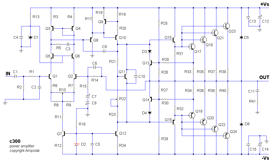
The c300 up close
This 300 Watts/RMS amplifier is meant for those who are not only looking for higher power, but superior performance as well. In order to achieve this, the c300 features some advanced techniques that are absent in its' smaller counterpart (c200).


Additions in 1st Gain Stage

Cascodes
Right at the very first gain stage, cascodes (Q5,6) are adopted. They serve to improve the high frequency performance of the c300. These cascodes are biased to approximately midpoint between 0V and +V by zener diode D1 (33V).

Current Mirrors
The first stage also contains current mirror Q3,4. As the name implies, the mirror forces equal current in the LTP (long tail pair). It is known for its' active loading and high gain properties.

Emitter Degeneration Resistors
Slew rate of the input differential is improved by resistors R6,7,8,9,10. In the absence of matched transistors, preset R10, is used for trimming DC to a minimum at the output of the amplifier.


Buffering the 2nd Stage

The VAS mod
The 2nd stage is direct coupled to the differential via a darlington Q8. This effectively buffers Q10, the main transistor that is amplifying the voltage from loading the preceding stage. Q10 is biased into class A by constant current source Q12. Capacitor C9 sets the dominant pole in Miller compensation.


Thermal Tracking

The remaining parts of the circuit is conventional. Vbe multiplier Q11, adjust the bias for the output transistors which is in full complementary EF configuration. Q11 must be thermally coupled to the main power heatsink for proper thermal tracking. VI Limiting network consists of Q13,14, R25~30 and D3,4. This network is optional, and can be omitted if desired.


THD of c300


Biasing of output transistors
All THD readings were done with outputs biased to 20mV across 0.39 ohms emitter resistor. This works out to approximately 55mA per output transistor in idling state.

Download High Res Schematics

Solid State Hybrid

As opposed to discrete designs, the IA502 uses an IC to drive the power stages.The entire power amplifier circuitry for 2-channels are squeezed into a tiny TDA7250 10-pin IC. All that's required are four power darlingtons and some passive components to complete a high performance stereo amplifier. No biasing is required as the IC auto biases the output transistors.The IA502 lends itself well to multi-channel amplification.A 6~8 channel power amplifier can easily be constructed even by beginners.

The TDA7250cfpThis 2-channel hybrid IC is normally configured with TIP142/147 power darlingtons for its' output. For those who prefer to use power transistors instead, the TDA7250 can easily be converted. All that is required are a few transistors, 4 additional resistors and some rewiring.This conversion centers mainly on changing the output section to a Sziklai.Sziklai Output In our IA502 on the right, drivers Q1,Q2 are 2SC2238 and 2SA968, and outputs Q5,Q6 are 2SA1216 and 2SC2922 respectively.No instability problems were encountered from this conversion. After a period of run-in, the amplifier remained thermally stable.Is this version worth the extra cost and effort?If one is only interested in something basic, the TIP version would be sufficient. But if one is after sonic performance, I would recommend this version.


170W Audio Power Amplifier Class D

With LM4651 & LM4652
The combination of the LM4651 driver IC and the LM4652 power MOSFET Class D power amplifier IC provides a high efficiency amplifier solution, suitable for self-powered speakers, subwoofers and quality car boosters.
The LM 4651 is a fully integrated conventional pulse width modulator (PWM) driver, containing undervoltage, short circuit, overmodulation, and thermal shutdown protection circuitry. The IC features a standby function which shuts down the pulse width modulation, minimizing supply current.
The LM 4652 is a fully integrated H-bridge Power Mosfet IC in a TO220 power package. The IC has a built in temperature sensor to alert the LM4651 when the die temperature exceeds the threshold limit.
Used together, the LM4651 and LM4652 form a simple, compact, efficient, high quality power audio amplifier solution complete with protection, normally seen only in Class AB amplifiers.
170 W POWER AMPLIFIER schematicThe maximum efficiency of this circuit is 85% at 125W with a standby attenuation greater than 100dB. The THD at 10W, 4 ohms, 10 - 500Hz is max. 0.3%. The supply voltage can not exceed ± 22V.
LM5651 Connection DiagramLM5652 Connection DiagramFor the best performance a suitable preamplifier is required. With the addition of a preamplifier the gain of the power stage can be greatly reduced to improve performance. The gain should be set to 10 V/V allowing for low gain on the Class D stage with a total system gain high enough to be a complete solution for line level sources.
The input filter used here does not noticeably increase THD performance but will help to maintain a flat frequency response as the Q of the output filter changes with load impedance.
Preamplifier and filter schematic with LM833 ICDesign notes, full specs and recommended PCB reference designs can be found here.
Do not attempt to build this amplifier as your first project! Class D high power amplifiers are expensive, difficult to build and a very small error during assembly can lead to total devastation of the power IC or other costly components.

Power Amplifier MOSFET 360 W

I propose here a more powerful version of the 200 Wrms 8 ohms AB class power amplifier project. It shares the same concept that the less poweful model : assembled using common compoments (not very expensive), based on traditional diagrams : a symmetrical differential input stage, a cascode stage driver and a MOSFET output stage.The printed circuit board is very compact , and is composed of two subsets : the command stage and the output stage.All resistors are 1/4 watt 1 % metal film (except if otherwise stated).Constant current sources of +/- 1 mA are formed around T5 and T6. The diodes D1 to D6 allow the use of low noise transistors type BC550C and BC560C, the transistors T7 to T10 form the stage driver. The potentiometer P1 allows the adjustment of the quiescent current to 100 mA per output transistor.The symmetrical power supply is entrusted to a large transformer of 750 VA, 2 * 60 volts + bridge rectifier and 8 reservoir capacitors of 4700 µF, which gives an output voltage of + and - 85 volts per rail. A 1000 VA transformer is necessary for maximal continuous output power at 4 ohms.The output power is 360 Wrms under 8 ohms or 550 Wrms under 4 ohms. Distortion is lower than 0,02 %, damping factor is better than 400, signal-noise ratio is 112 db (balanced A at full power), the input sensitivity is 1,2 volts (360 W under 8 ohms).

Diagram : 

The capacitor C3 is not reproduced on the diagram and on the PCB (it is correct).

Proposal of the command stage PCB : 
 
Transistors T9 and T10 must be assembled on a common heatsink with 5° c/w thermal resistance or on the output stage heatsink.

Proposal of the output stage PCB : 

 The points marked A, B and C have to be connected between the two PCBs.The ground (earth) points of PCBs and loudspeaker ground (earth) must compulsorily be connected in star with the 0 Volts of the PSU.The power transistors must be assembled on a heatsink with a termal resistance less than 0.5 ° C/W. They must also be electrically insulated from the heatsink by using a mica insulator + heat-conducting compound or a silicone insulator.

Bandwidth : 
Bandwidth is limited from 5 Hz to 53 Khz (at - 3 db) by the input module (C1, R1, C2, R2). It can be modified according to the application desired. It is useless to increase the bandwidth to the botton (bass) because little useful signal is present at the bottom of the spectrum. In public address sound systems the bandwidth is often limited between 20 and 35 Hz. The loudspeakers are thus protected against too high extreme-bass signals and some more power is available for the remainder of the spectrum. Michael Eveleigh (UK)
 Source : http://users.swing.be/edwinpaij/ampli_mosfet_360_w.htm

THE LEACH SUPERAMP 270 W

This amplifier is the monophonic 270 watt Double barreled Amplifier. For the original article, I specified plus and minus 85 V dc power supply voltages. The voltage can be increased to about 93 V to obtain a power rating of 300 W. The amplifier can be built either as a stereophonic or a monoponic unit. My original amps were mono units because the heat sinks, transformer, and filter caps that I used were too large for a stereo amp. The circuit described on this page is a modification of the original Double Barreled Amplifier. The circuit has been simplified somewhat. The circuit board layout is smaller and much more compact. The driver transistors now mount on the circuit board instead of on external heat sinks. And the circuit has the feedforward compensation that I describe for the Low TIM Amplifier. If you build this amplifier, you must keep the wiring between the heat sinks and the circuit boards as short as possible if you don't want oscillation problems. When you test the circuit boards before connecting the power transistors, temporarily connect a 10 ohm resistor in series with a 0.1 ufd capacitor from the loudspeaker output to the power supply ground.


The Circuit Boards
I do not have circuit boards for the Double Barrelled Amplifier. If you wish to build it, you must make your own. Two drawings show the parts layout on the board, one with circuit traces and one without. These are scaled by a factor of 1.5. The other shows the circuit traces only. All layout views are from the component side of the board. You must flip the layout for the foil traces over to obtain the solder side view. The circuit board measures 4 inches by 6 inches. To my knowledge, there are no errors in the layout. If you decide to use it, you should carefully check it for errors because I could have easily made a mistake. I do not recommend that you make the circuit boards unless you have experience in doing it. A source of materials for making your own printed circuits can be found here. I have been told that their "Press and Peel Blue" product (not the wet stuff they sell) can be used to successfully make boards with traces as narrow as 0.01 inch. The smallest traces on the amplifier layout are 0.03 inch wide. The PnP Blue product is basically a transfer medium that allows you to transfer the toner image from a laser printer directly onto bare copper clad board and then etch it in FeCl3 (ferric chloride). After you etch the board, the copper should be cleaned with steel wool, lightly coated with solder flux, and then "tinned" with a soldering iron and rosin core solder. Do not use a commercial tinning solution that you dip the board into. It is almost impossible to solder a board that is tinned with one of these products because they corrode very quickly. When you drill the board, you should use the correct size drill bit for the pads. The hole diameters I recommend are: small pads - 0.032 inch, medium pads - 0.040 inch, large pads - 0.059 inch, mounting holes - 0.125 inch. If you do not use a sharp drill bit, you can pull the pads off the board when you drill it.

Circuit Description
If you compare the Double Barreled circuit to the Low TIM circuit, you will see a lot of similarity between the two. Indeed, there is a Low TIM Amplifier embedded in the Double Barreled Amplifier. The major difference between the two is that transistors are added in series with those in the Low TIM circuit to form the Double Barreled circuit. By doing this, the voltage across the transistors is decreased so that the power supply voltage can be increased for higher output power. Basically, the circuit description for the Low TIM Amplifier also applies to the Double Barreled Amplifier. The major difference between the two is the addition of transistors Q22 through Q31. Q22 is connected as a common base stage at the output of Q12. The two transistors form a cascode stage. The base of Q22 connects to the junction of R52 and R54. These two resistors are equal and are connected as a voltage divider between the loudspeaker output and the positive rail. This forces the base voltage of Q22 to float half way between the loudspeaker output voltage and the positive power supply rail. Similarly, Q13 and Q23 form a cascode stage. R53 and R55 force the base of Q23 to float half way between the loudspeaker output voltage and the negative power supply rail. The addition of Q22 and Q23 cause the collector to emitter voltages of Q12 and Q13 to be approximately one-half of what the voltages would be without Q22 and Q23. Transistors Q24 and Q25 connect in series with the pre-driver transistors Q14 and Q15. The base of Q24 floats half way between the output voltage and the positive rail. The base of Q25 floats half way between the output voltage and the negative rail. The addition of Q24 and Q25 cause the voltages across Q14 and Q15 to be approximately one-half of what they would be without Q24 and Q25. Similarly, transistors Q26 through Q31 cause the voltages across Q16 through Q21 to be approximately one-half of what they would be without Q26 through Q31. By connecting the transistors in series in this way, the rail voltages can be increased for higher output power. The basic construction details of the Low TIM Amplifier also apply to the Double Barreled Amplifier. There are two short circuit jumper wires that must be soldered on the circuit board. These are marked with a J on the layout. In addition, you must solder a short circuit jumper in place of C6B if you use a non-polar capacitor for C6A. This is explained in the parts list for the Low TIM Amplifier. Because there are eight output transistors, two main heat sinks per channel are required. Q18, Q20, Q28, and Q30 should be mounted on one and Q19, Q21, Q29, and Q31 on the other. Resistors R61 through R64 and wires connecting the collectors of Q18 and Q20 and the collectors of Q19 and Q21 mount on the heat sinks. These connect between lugs on the transistor sockets. The four bias diodes D1 through D4 can be mounted on either heat sink. It is not necessary to divide the diodes between the two heat sinks because both heat sinks will operate at the same temperature. I recommend setting the voltage across Q7, i.e. the voltage between the collectors of Q22 and Q23, so that that amplifier is biased at 120 mA. This will give the same quiescent power dissipation per heat sink as in the Low TIM Amplifier.

Testing the Circuit Boards
After you solder the parts to the circuit board, it is tested using the same procedure specified for the Low TIM circuit board. First, you must solder the short circuit jumper across Q7 and you must solder the 100 ohm 1/4 W resistors from the loudspeaker output to the emitters of Q16 and Q17. If you don't have a bench power supply that puts out plus and minus 85 to 93 V dc, you can test the circuit board at a lower voltage. I would prefer test voltages of at least plus and minus 50 V dc. An option is to connect bench power supplies in series to obtain the plus and minus 85 to 93 V dc. I have routinely connected two 40 V Hewlett Packard power supplies in series with the positive and negative outputs of a Hewlett Packard 50 V dual power supply, and I have never had any problems. To protect the circuit boards, you might want to put a 100 ohm 1/4 W resistor in series with the plus and minus power supply leads for the tests. The current drawn by the circuit should be low enough so that the voltage drop across these resistors is less than 1 V if nothing is wrong on the circuit board. There are 2 ground wires from the circuit board. Both must be connected when testing the boards. I can't stress how important it is to be careful in testing a circuit board. Even simple errors can cause the loss of many expensive transistors. I always use current limited bench power supplies to test a circuit board before and after connecting the power transistors. I also bias an amplifier using current limited power supplies in place of the amplifier power supply. When I initially power up an amplifier with its own power supply, I always use a Variac variable transformer to slowly increase the ac input voltage from 0 to 120 V rms while observing the amplifier output on an oscilloscope with a sine wave input signal. If I see anything wrong on the oscilloscope, I turn the Variac to zero and try to diagnose the problem using the bench power supply. I never use a load on the amplifier for these tests.

Parts List
With the following exceptions, the parts for the Double Barreled Amplifier are the same as for the Low TIM Amplifier.
Capacitors
C10, C11 - 15 pF mica
C13, C14 - 100 uFd 100 V radial electrolytic
C21, C22 - 47 uFd 100 V radial electrolytic
C26, C27 - 270 pF mica
C28 - 0.01 uFd 250 V film
Transistors
Q1, Q2, Q5, Q7, Q9, Q10 - MPS8099 or MPSA06
Q3, Q4, Q6, Q8, Q11 - MPS8599 or MPSA56
Q23, Q24 - 2N3439
Q22, Q25 - 2N5415
Q26 - MJE15030
Q27 - MJE15031
Q28, Q30 - MJ15003
Q29, Q31 - MJ15004
Diodes
D5, D6 - 1N4934 fast recovery rectifier
D13 through D16 - 1N5250B 20 volt zener diode
Resistors
R13, R14 - 5.6 kohm 1 watt (This value is for 85 V power supplies. For other power supply voltages, the formula is on the Parts List page for the Leach Amp.)
R28, R29 - 200 ohm 1/4 watt
R30, R31 - 3.9 kohm 1 watt
R37 through R40 - 470 ohm 1/4 watt
R41 through R44 - 10 ohm 1/2 watt (changed 6/27/00)
R52 through R55 - 6.2 kohm 1 watt
R56 through R59 - 10 ohm 1/2 watt (changed 6/27/00)
R60 - 39 ohm 1/4 watt
R61 through R64 - 0.33 ohm 5 watt. These 4 resistors are mounted on the heat sinks between solder lugs on the power transistor sockets. The wires that connect the collectors of Q18 and Q20 and the collectors of Q19 and Q21 are also soldered between the lugs on the sockets. Keep all leads as short as possible and use insulation stripped from hookup wire around the bare leads of the resistors.
R65, R66 - 300 ohm 1/4 watt

Download :

Audio Amplifier MOSFET 200 W

Here is propose a project ofan AB class power amplifier, at its simplest, assembled with common compoments(not very expensive), based on traditional diagrams : a symmetricaldifferential input stage, a cascode stage driver and a MOSFET output stage.
The printed circuit board isvery compact , and is composed of two subsets : the command stage and theoutput stage. All resistors are 1/4 watt 1 % metal film (except if otherwisestated).
Constant current sources of+/- 1 mA are carried out around T5 and T6. The diodes D1 to D6 allow the use oflow noise transistors type BC550C and BC560C, the transistors T7 to T10 formthe stage driver. The potentiometer P1 allows the adjustment of the quiescientcurrent to 100 mA per output transistor.
The symmetrical power supplyis entrusted to a large transformer of 625 VA, 2 * 51 volts + bridge rectifierand 6 reservoir capacitors of 4700 µF, which gives an output voltage of + and -70 volts per rail.
The output power is 200 Wrmsunder 8 ohms or 350 Wrms under 4 ohms. Distortion is lower than 0,02 %, dampingfactor is better than 300, signal-noise ratio is 112 db (balanced A at fullpower), the input sensitivity is 1,2 volts (200 W under 8 ohms).

Diagram :
The capacitor C3 is notreproduced on the diagram and on the PCB (it is correct).

Proposal of the command stage PCB :

Transistors T9 and T10 mustbe assembled on a common heatsink with 5° c/w thermal resistance or on theoutput stage heatsink.

 proposal of the output stage PCB :

The points marked A, B and Chave to be connected between the two PCB.
The ground (earth) points ofPCB's and loudspeaker ground (earth) must compulsorily be connected in starwith the 0 Volts of the PSU.
The power transistors mustbe assembled on a heatsink with a thermal resistance less than 1 ° C/W. Theymust also be electrically insulated from the heatsink by using a mica insulator+ heat-conducting compound or a silicone insulator.
It is possible to use theMOSFET output stage PCB which is also reproduced on the site, but take carewith the thermal dissipation of the output transistors (this circuit is perfectfor power of 100 Wrms under 8 ohms or 155 Wrms under 4 ohms). It is possible touse two PCBs in parallel to double the number of output transistors, do notplace the limitation diodes, the fuses and the RC output circuit on the secondPCB.

Bandwidth :
Bandwidth is limited from 5Hz to 53 Khz (at - 3 db) by the input module (C1, R1, C2, R2). It can bemodified according to the application desired. It is useless to increase thebandwidth to the botton (bass) because little useful signal is present at thebottom of the spectrum. In public address sound systems the bandwidth is oftenlimited between 20 and 35 Hz. The loudspeakers are thus protected against toohigh extreme-bass signals and some more power is available for the remainder ofthe spectrum.
Source : http://users.swing.be/edwinpaij/ampli_mosfet.htm monggo dipun klik mawon

100W LM3886 Parallel Stereo Power Amplifier

This amplifier is based on the PA100 parallel amplifier detailed in National Semiconductor's application note - AN1192. Since my DIY speaker is 4-ohm and somewhat difficult to drive, I want to have a more powerful amplifier to match with it. Therefore I designed this amplifier which uses two LM3886 per channel, in parallel circuit. This amp can deliver about 50W into a 8-ohm speaker and 100W into a 4-ohm speaker. This is a stereo amplifier and therefore 4 LM3886s are used. The LM3886 circuit is in a non-inverted configuration, so the input impedance is determined by the input resistor R1, i.e. 47k. The 680 ohm and 470pF resistor capacitor filter network is used to filter out the high frequency noise at the RCA input. The 220pF C4 and C8 capacitors are used to shot out the high frequency noise at the LM3886 input pins. I used high quality audio grade capacitors at several locations: 1uF Auricap at the input for DC blocking, 100uF Blackgate for C2 and C6, and 1000uF Blackgate at the supply filter.

100W LM3886 Parallel Stereo Power Amplifier

The PCB is designed in a way that the power ground is separated from the signal ground, as you can see from the below layout. The signal ground is located in the middle and surrounded by the power ground. There is a thin trace near C5 connecting them. The PCB layout is done by using PADS PowerPCB 5.0. I think it is a powerful layout software. After finished the layout, I send it to a PCB manufacturer in HK to make the PCB. After the PCB is made, I found some of the drill holes are not large enough.... I have to make it bigger manually.
Finished PCB.

The 20k and 1k resistors are hand matched to 0.1%. For the output resistors, I used six 0.5W 1% 1ohm resistors in parallel per 3886 output instead of one 3W resistor because 3W 1% resistors are hard to find.

I used the insulated version - LM3886 TF, so that I can mount it directly to the case and heat sink with thermal compound.


Coupling capacitor is Auricap 1uF 450V. I used this high quality capacitor because it is in the main signal path.

The HF filter capacitors are Silver Mica 47pF and 220pF.

The power supply filter used is Blackgate 1000uF 50V.

C2 and C6 are Blackgate 100uF 50V. For better result, the bi-polar version should be used. However I am not using it because the bi-polar blackgate is too big to fit into my PCB.

The 680 ohm + 470pF filter network is installed at the RCA. This help filtering the high frequency noise before it gets onto the board.

The WIMA 0.1uF supply decoupling capacitors are soldered directly on the pins of LM3886 at the back of the PCB. This helped to remove some high frequency noise.

The 3886 are mounted on a 3/8 inch aluminum plate then to the case. Outside of the case I used 3 PC CPU heatsinks. I used Arctic Silver thermal compound between the aluminum layers to improve heat conductivity.

With all these big heatsinks, it only get slightly warm when listen at normal volume.

The power supply used is a regulated power supply. I used 10000uF per rail before the LT1083 regulator. After the regulator, I have 100uF on the regulator board. The advantage of using regulator is that the power supply ripple voltage is removed. If power regulation is not used, I can hear very little 50/100Hz hum from the speaker.


Power Supply Schematic :


The high current MUR860 diode is used to ensure high current flow.


The voltage regulator used is LT1083, it can provide about 8A of current.

Transformer used here is a 500VA 2x 25V. The power supply is then regulated by 2 LT1083, after the regulation, the voltage is 30V.


Will consider to use this supply circuit instead, the TIP2955 is capable of providing 15A of current:

I did some DC measurement and the result is quite good, I got 7 mV of DC offset at the speaker terminal. The voltage difference between the output of the 2 chips is less then 1 mV.

The sound of this amplifier is similar to my LM3875 amplifier, which is very clean and detail. It has no hum, no hiss and no noise. Compared to the LM3875 Gainclone, this amp can deliver twice the power to my 4-ohm speaker, and it improves the dynamics and bass punch a lot.


100W LM3886 Parallel Stereo Power Amplifier


100W LM3886 Parallel Stereo Power Amplifier


100W LM3886 Parallel Stereo Power Amplifier

100W LM3886 Parallel Stereo Power Amplifier

100W LM3886 Parallel Stereo Power Amplifier

100W LM3886 Parallel Stereo Power Amplifier

100W LM3886 Parallel Stereo Power Amplifier

100W LM3886 Parallel Stereo Power Amplifier

100W LM3886 Parallel Stereo Power Amplifier

100W LM3886 Parallel Stereo Power Amplifier